How Dental X-Ray Sensors Work
An exhaustive engineering analysis detailing architectural layer configurations, conversion formulas, and deep data pathways that dictate exactly how dental x-ray sensors work.
⏱️ 15-18 min read
✓ Technical Standards Compliant
⚡ Core Engineering Executive Summary
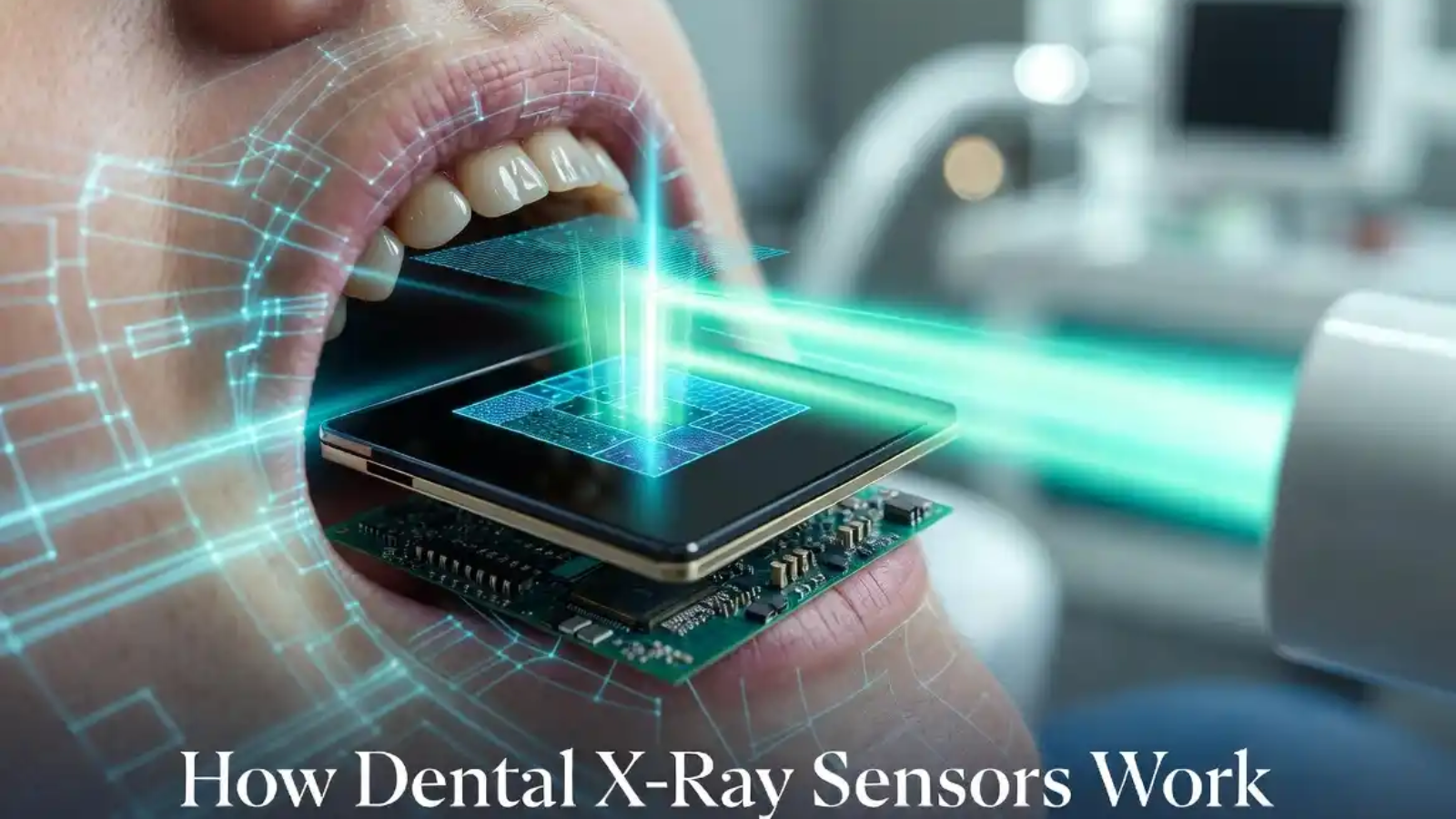
Understanding how dental x-ray sensors work requires isolating a sequence of three technical changes. Before diving into pixel arrays, it is best to review the core architecture in our guide: What Is a Dental X-Ray Sensor? High-voltage tungsten emission penetrates dental tissue and strikes an active Cesium Iodide (CsI) scintillator substrate, which instantly maps incoming shortwave ionizing energy into uniform visible light bands. Next, these light packets are guided by an integrated fiber-optic plate onto a solid-state CMOS or CCD semiconductor wafer, inducing a localized photoelectric current that traps electron concentrations proportional to tissue density. Finally, an on-chip Analog-to-Digital Converter (ADC) maps these variations into binary signals, outputting an ultra-sharp, high-resolution diagnostic image to imaging software suites via high-speed USB paths in milliseconds.
Table of Contents
1. Solid-State Physics and Quantum Dynamics
To systematically analyze how dental x-ray sensors work, one must evaluate the mathematical and quantum interactions occurring when ionizing electromagnetic radiation meets dense atomic elements. Unlike classical analog film systems that rely on slow chemical silver-halide suspension reactions, modern intraoral sensors operate entirely on photoelectric conversion mechanics. The process involves tracking high-energy photons emitted by an x-ray tubehead—typically operating within a calibrated parameters spectrum of 60 kVp to 70 kVp and an anodic current of 4 mA to 7 mA.
As these highly energized photons penetrate the oral cavity, they undergo attenuation variations determined directly by the material’s atomic number and localized density. Highly mineralized tooth structures (hydroxyapatite enamel matrices) absorb the massive majority of the x-ray photons through complete photoelectric absorption. Conversely, less dense pathways—such as active pulp chambers, initial interproximal decay networks, and periodontal ligament gaps—allow the photons to pass through with minimal speed losses. The spatial density map produced by this pattern strikes the active face of the sensor, establishing the foundational parameters for high-definition digital processing.
2. Deep Micro-Layer Structural Anatomy
Evaluating how dental x-ray sensors work requires looking past the protective outer casing. The external body is typically composed of impact-resistant polycarbonates or thermoplastic polyurethanes designed to withstand saliva exposure, chemical disinfectants, and patient biting pressures. Inside this protective outer box sits an intricately layered diagnostic sandwich:
1. Scintillator Screen Matrix
The frontline diagnostic component, commonly crafted using micro-crystalline Cesium Iodide (CsI) doped with Thallium, or Gadolinium Oxysulfide. Because standard silicon substrates possess very low absorption properties for raw x-ray wavelengths, the scintillator acts as a crucial first-step converter. Its needle-like micro-structures act as highly efficient fiber-optic pipes, capturing incoming x-ray photons and immediately converting them into concentrated bursts of visible light spectrum waves (typically around 550nm).
2. Coherent Fiber-Optic Plate (FOP)
A dense, multi-million fiber element positioned directly beneath the scintillator screen. This layer fulfills two critical purposes: it guides the converted visible light paths directly down to the silicon surface without allowing side-to-side scatter (preserving edge resolution and clarity), while actively blocking unabsorbed x-ray photons from reaching and degrading the sensitive underlying logic chips.
3. Solid-State Imaging Semiconductor
The structural core of the digital asset, leveraging either highly customized Complementary Metal-Oxide Semiconductor (CMOS) arrays or heritage Charge-Coupled Device (CCD) structures. This thin silicon wafer contains millions of independent pixel wells that compile and hold localized electrical charges proportional to the light intensity striking them.
4. Shock-Absorbing Core & Electronic Shielding Substrate
At the base of the structural sandwich sits a heavy-metal lead back-shielding plate. This layer prevents backscattered radiation from creating image noise, while an embedded anti-shock damping pad isolates the brittle silicon wafer from sudden drops or strong biting forces.
3. Microsecond Processing & Readout Sequence
The transition from an explosive burst of sub-atomic particles to an accurate digital diagnosis on an operatory monitor follows a strictly timed engineering process. This operational sequence dictates exactly how dental x-ray sensors work across every single exposure run:
The tubehead releases a targeted stream of x-ray photons. As they pass through tissue and reach the faceplate, the internal scintillator layer absorbs this invisible energy, instantly transforming it into green or blue visible light bands directed downward toward the semiconductor matrix.
The newly transformed light photons pass through the fiber optic plate and hit the silicon semiconductor. This interaction triggers an internal photoelectric phenomenon: photons knock electrons free within the silicon matrix, creating electron-hole pairs that collect inside the capacitive pixel wells. The number of trapped electrons forms an analog charge map that directly reflects the patient’s anatomical variations.
An integrated Analog-to-Digital Converter (ADC) sweeps across the pixel matrix. In CMOS setups, miniature transistors at every individual pixel well amplify and convert the analog voltage value into clean binary data paths instantly. This digital conversion assigns specific numerical color codes across a 256 to 4,096 grayscale hierarchy, depending on the sensor’s bit depth.
The raw digital packets travel up a heavily shielded high-speed USB cable (or via wireless Bluetooth/Wi-Fi modules) directly to the server terminal. Companion software suites apply real-time filtering matrices to balance contrast and noise, displaying a crystal-clear diagnostic image on the monitor in under three seconds.
4. SwatDental Engineering & Learning Library
To expand your baseline master configuration beyond analyzing how sensors record localized energy maps, explore our specialized engineering background logs. Building a complete procedural understanding helps operatory teams resolve image anomalies and hardware faults instantly:
What Is a Dental X-Ray Sensor?
Need a comprehensive look at basic tubehead physics, anode targets, and focal spot geometry? Read our diagnostic breakdown to master the raw source mechanics before learning how sensors catch the beams.
Intraoral Sensor Size Procurement Guide
Now that you know the internal micro-layer layout of a semiconductor wafer, learn how physical active dimensions change across Size 0, Size 1, and Size 2 architectures to match specific patient anatomy footprints.
5. Advanced Spatial Resolution & Specification Profiles
When evaluating sensor hardware for an operatory setup, clinical teams must analyze several interconnected performance criteria. These engineering specifications determine the absolute limits of your diagnostic capabilities:
Measured in line pairs per millimeter (lp/mm). Premium sensors offer a theoretical limit of >25 lp/mm, with a visible resolution limit of 14 to 20 lp/mm. This high density allows clinicians to accurately trace micro-fractures, secondary decay lines, and structural shifts along implant boundaries.
Refers to the actual physical size of individual pixel wells on the silicon chip. High-tier diagnostic sensors keep this spacing between 18.5 to 22 micrometers. Tighter pixel pitches yield significantly higher spatial data resolution thresholds, which is essential for detecting early bone loss patterns.
Measures how effectively a system turns incoming radiation energy directly into valid pixels. Solid-state sensors achieve excellent efficiency marks of 40% to 70%, allowing clinics to slash patient radiation exposure numbers by up to 80% compared to legacy film options.
Quantifies the sensor’s capability to transfer contrast from a physical object over to the final digital screen file at varying spatial frequencies. High MTF ratings prevent fine structures from becoming blurry or washed out.
Leverages high-bit processing channels (12-bit up to 16-bit configurations) to capture thousands of unique gray values, highlighting tiny changes in bone density.
High-end hardware optimizes SNR by keeping background noise thresholds safely below 200 electrons. This reduction eliminates graininess, delivering clean, artifact-free visual files across standard operational cycles.
6. Silicon Readout Systems: CMOS vs. CCD
While both semiconductor platforms capture incoming light rays successfully, the architectural mechanics defining exactly how dental x-ray sensors work vary heavily between CMOS and CCD architectures. Understanding these readout differences is critical for procurement planning:
| Engineering Feature | CMOS Sensors (Complementary Metal-Oxide) | CCD Sensors (Charge-Coupled Device) |
|---|---|---|
| Signal Amplification Architecture | Individual transistors located inside every single pixel node amplify signal tracks independently. | Charges shift across pixel rows sequentially to a single dedicated readout node for amplification. |
| Data Generation Velocity | Ultra-fast parallel data streams deliver image views on monitors in under 1.5 to 2 seconds. | Slower sequential data processing can introduce a minor display lag (3 to 5 seconds). |
| Power Metrics & Mobility | Extremely low energy requirements, allowing for sleek, true wireless connectivity systems. | Higher power draw requirements, generally necessitating a continuous, physical wired USB link. |
| Structural Profile Limits | Thinner base footprint, significantly improving patient comfort parameters. | Thicker, rigid casing profiles due to specialized sequential tracing designs. |
| Manufacturing Yield & Economics | Produced on standard silicon assembly lines, reducing replacement costs for clinics. | Requires dedicated fabrication facilities, resulting in a premium capital expenditure. |
7. Clinical Specialization & Diagnostic Integration
Analyzing how dental x-ray sensors work highlights huge practical advantages for daily clinical workflows. Moving past slow physical development processes unlocks several operational benefits:
🔬 Precision Endodontics
Essential for tracking working root length. Instant display settings let operators monitor files in real-time during apex configuration tasks, trace calcified root blockages, and confirm final canal seal completeness.
🦷 Operative Dentistry
Provides crisp, detailed bone tracking views to assess micro-leakage risks under complex crown assemblies, check cavity margins before placing materials, and verify deep structural soundness.
🦴 Periodontal Monitoring
Delivers ultra-precise mapping data to track horizontal or vertical alveolar bone loss patterns, monitor tricky furcation involves, and evaluate bone regeneration progress after osseous surgery.
👶 Pediatric Adaptability
Significantly lowers radiation exposure levels for younger, developing tissues. Rounded size-0 dental x-ray sensor shapes fit safely inside smaller mouths, while instant image rendering eliminates patient movement artifacts.
For official global technical compliance metrics and sensor testing protocols, review the
FDA Radiation-Emitting Products Directives
and explore the diagnostic safety recommendations detailed by the
American Dental Association (ADA) Science Center.
8. Frequently Asked Questions
Why can’t raw silicon chips process x-rays directly without a scintillator?
Raw silicon substrates are largely transparent to high-frequency, short-wavelength x-ray photons, meaning most radiation passes through without leaving an electrical charge. An internal scintillator layer acts as a crucial middle step, capturing raw x-rays and transforming them into visible light, which the silicon pixel wells can then easily detect and process.
Does the internal light conversion step blur the final diagnostic picture?
No, because modern systems feature an integrated fiber-optic plate behind the scintillator. This micro-structural layer uses thousands of parallel glass fibers to guide light beams directly down to the pixel wells without any side-to-side scatter, keeping the final image crisp and clear.
What causes digital x-ray images to degrade over long periods of use?
Image degradation is usually tied to physical cord strain or cumulative radiation damage, known as ionizing browning. Using protective positioners and handling cables carefully ensures your solid-state sensors deliver consistent, high-resolution diagnostic performance for years.
Final Technical Summary
Understanding how dental x-ray sensors work underscores the incredible blend of physics and engineering supporting modern dentistry. Transitioning from chemical developer tanks to high-efficiency solid-state CMOS and CCD sensors drastically lowers patient exposure risks while delivering instant, ultra-high-resolution diagnostic files. By utilizing scintillators, fiber optics, and advanced analog-to-digital converters, modern intraoral sensors capture hidden path patterns in seconds, streamlining clinical workflows and elevating long-term practice performance.
Add a Comment
Logged in as wad_ant
Ready to upgrade your clinical workflow? Explore premium imaging setups and diagnostic sensor configurations at
SwatDental.
Add a Comment